Leading ‘Silicon Module Super League’ (SMSL) member JinkoSolar has set further records by establishing new P-type and N-type PV module power ratings ahead of the largest annual industry exhibition, SNEC in Shanghai, China.
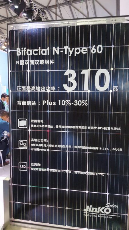
JinkoSolar said that it had set the record for a P-type monocrystalline module (60-cell) format peak power rating of 370W and an N-type monocrystalline module (60-cell) format peak power rating of 378.6W.
Unlock unlimited access for 12 whole months of distinctive global analysis
Photovoltaics International is now included.
- Regular insight and analysis of the industry’s biggest developments
- In-depth interviews with the industry’s leading figures
- Unlimited digital access to the PV Tech Power journal catalogue
- Unlimited digital access to the Photovoltaics International journal catalogue
- Access to more than 1,000 technical papers
- Discounts on Solar Media’s portfolio of events, in-person and virtual
Or continue reading this article for free
Both records were said to have been verified by TUV Rheinland (Shanghai) Co., Ltd.
Dr. Jin Hao, Vice President of JinkoSolar commented, “Every technological breakthrough results from a strong pioneering spirit and constant search for excellence. Companies with strong independent innovation capabilities are able to grasp opportunities in fiercely competitive markets and establish leadership. JinkoSolar always applies advanced technologies to large-scale applications rapidly to accelerate the popularization of PV applications.”
The company noted that its P-type mono modules contain JinkoSolar's world record high-efficiency cells, which combined with low electricity loss technology reduces the module internal resistance and improves its fill factor to achieve the new performance record.
The N-type modules were said to use dual glass, deploying passivating contact technology to achieve high efficiency with front-side peak power reaching 378.6W.
JinkoSolar has recently reset the P-type monocrystalline cell conversion efficiency record at 23.95%, through a range of wafer to cell optimisation, notably its selective emitter (SE) formation.


