
According to Bernreuter Research, polysilicon consumption for the production of solar wafers is set to impact the supply-side as the PV industry adopts diamond wire technologies that significantly lower kerf loss.
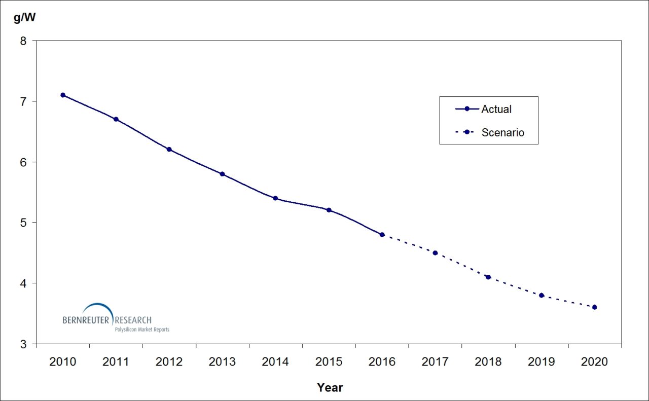
Bernreuter Research said that the average silicon consumption for the manufacturing of both multicrystalline and monocrystalline wafers was expected to decline from 4.8 grams per watt (g/W) in 2016 to 3.6 g/W in 2020, a 25% decline.
Unlock unlimited access for 12 whole months of distinctive global analysis
Photovoltaics International is now included.
- Regular insight and analysis of the industry’s biggest developments
- In-depth interviews with the industry’s leading figures
- Unlimited digital access to the PV Tech Power journal catalogue
- Unlimited digital access to the Photovoltaics International journal catalogue
- Access to more than 1,000 technical papers
- Discounts on Solar Media’s portfolio of events, in-person and virtual
Or continue reading this article for free
A key driver is resurgence in using monocrystalline wafers that offer higher sola cell conversion efficiencies but have also undertaken significant cost reductions to make the technology increasingly competitive with multicrystalline wafers that have dominated the sector for the last 10-years.
The increased demand for monocrystalline wafers was recently highlighted by Finlay Colville, head of solar intelligence at Solar Media in a PV Tech blog, forecasting that mono c-Si cell production is forecast to account for 49% of all c-Si cell production in 2018, and will become the dominant technology used in the PV industry by 2019.
Echoing that forecast, Bernreuter Research expects the market share of mono c-Si wafers to increase from 27% in 2016 to 47% in 2020.
Cost reductions have occurred across mono c-Si ingot and wafer production in recent years, yet the adoption of diamond wire cutting has been critical as it does not require expensive slurry and can be produced with thinner wires, minimising kerf loss and overall production costs.
However, multi c-Si wafer production is also expected to widely adopt diamond wire cutting and adopt newly developed wafer texturing technologies that will enable the migration, further supporting a drop in silicon consumption.
Bernreuter Research noted that the multi c-Si wafer production migration to diamond wire cutting and ‘black silicon’ texturing would take four to five years, accounting for around 90% of multi c-Si wafer production in that timeframe.
“The polysilicon industry has to prepare for the fact that demand is slowing down on two fronts: The annual growth rate of global photovoltaic installations is decreasing, and the polysilicon consumption for each new gigawatt installed in 2020 will be only half as much as it was in 2010,” noted Johannes Bernreuter, head of Bernreuter Research and author of the ‘Polysilicon Market Outlook 2020’.


