Trade body, VDMA has made key updates to the 10th edition of the International Technology Roadmap for Photovoltaics (ITRPV) to incorporate the ongoing and rapidly changing wafer size transition as well as the manufacturing throughput differences in front-end and back-end processes.
Dr. Markus Fischer of Q-CELLS R&D department and key ITRPV author, presented the update of the roadmap and the current maturity of a range of front-end and back-end processes, which includes the level of technology maturity, at the 10th Solar World Congress in Shanghai.
Unlock unlimited access for 12 whole months of distinctive global analysis
Photovoltaics International is now included.
- Regular insight and analysis of the industry’s biggest developments
- In-depth interviews with the industry’s leading figures
- Unlimited digital access to the PV Tech Power journal catalogue
- Unlimited digital access to the Photovoltaics International journal catalogue
- Access to more than 1,000 technical papers
- Discounts on Solar Media’s portfolio of events, in-person and virtual
Or continue reading this article for free
As PV Tech has highlighted in detail, solar wafer sizes across p-Type multicrystalline, p-Type monocrystalline, p-Type mono-cast and n-Type monocrystalline are rapidly transitioning to a number of larger wafer sizes, impacting the complete supply chain for the PV industry.
In the ITRPV update, only wafer sizes smaller than the M4 standard can be implemented in existing cell processing lines without incurring major modifications.
However, the M2 wafer (156.75 x 156.75) size has become the mainstream choice for many cell and module producers, not only for the limited equipment upgrades but also limiting module dimension, including weight) increases and providing legacy options for the future as well as fitting existing mounting systems.
With the M2 wafer increasing the module power by more than 5Wp, other leading companies looking for higher gains have adopted M6 and are also migrating to larger versions (M12) over the next few years. These require new production lines and for some leading manufacturers newly announced capacity expansion plans are designed specifically for the super large wafer sizes.
The old 6” format (156mm x 156mm) is expected to almost disappear completely from the market by the end of 2019.
Starting with M4 wafer size, an implementation is only possible with upgrades of existing lines, while new lines are required for the installation of wafers with sizes M6 and larger, according to the updated roadmap.
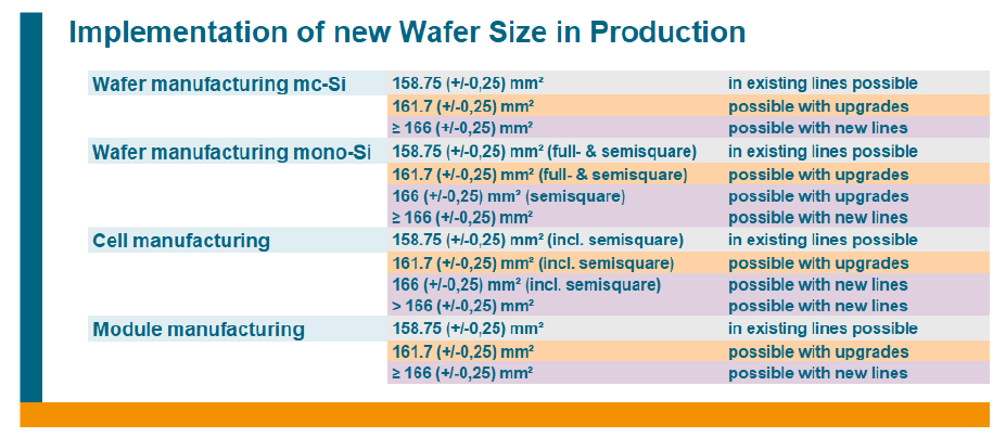
This trend is consistent in the production of mono- and multicrystalline silicon wafers as well as in cell and module production, according to the updated roadmap.
Not surprisingly, the roadmap notes the need for renewed standardization of wafer sizes as this creates cost issues for wafer cell and module processing equipment and automation suppliers having to provide bespoke solutions.
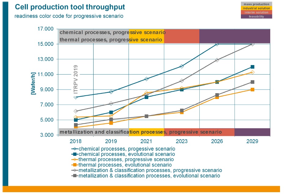
Processing equipment suppliers are also challenged with continuing throughput differences in front-end and back-end processes.
The annual survey of technology maturity for various selected parameters in the manufacturing of crystalline silicon solar cells, included in the ITRPV update, a large difference in the potential throughput has been observed.
The throughput of nearly 9000 wafers per hour in the front-end processes (chemical and thermal) is expected to be implemented in 2021 without major adjustments in mass production. This highlights that throughput differences will remain an issue.