Cell Processing

Premium
Cell Processing, Photovoltaics International Papers
According to the ITRPV (International Roadmap for PV), a large fraction of future solar cells will be n-type and rear-contact cells with the highest efficiencies and fabricated using low-cost processes. As the standard p-type silicon solar cell in mass production is completely optimized and has therefore reached its cost limit, it is currently very difficult for new solar cell concepts to be cost effective from the outset when introduced into production. Consequently, in the current market situation, the introduction of new solar cell concepts to the market is not straightforward. The only way to achieve this is to use the fully adapted standard processes employed in today's manufacturing lines and only upgrade them with a few industrially approved process steps – such as laser ablation and boron diffusion – in order to implement low-cost device structures with stable efficiencies well above 20%. This paper gives an overview of n-type cell concepts already present on the market and of promising technologies ready for pilot production; the latter were summarized and discussed at the 3rd nPV workshop in April 2013 in Chambéry, France. The consequences for module manufacturing, as well as for measurement techniques and for requirements in respect of new standardization for cell and module characterization, will also be discussed..
Premium
Cell Processing, Photovoltaics International Papers
Despite considerable progress in screen-printing processes for crystalline silicon solar cell metallization, alternatives are still of interest because of their potential cost and performance advantages. Plating processes are one alternative that can be either combined with printed seed layers or used for full front-contact deposition. Although there are advantages to both approaches, there are also challenges that must be faced. Plating nickel and copper onto printed seed layers is very simple and involves only minor process modifications. With regard to undesired paste–electrolyte interaction, noticeable progress has been made during the past few months, bringing this process closer to industrial implementation. Plating nickel directly onto silicon offers the possibility of contacting emitters even with a surfacedoping concentration as low as 8×1018cm-3, while achieving similar performance to that of an evaporated contact metallization. To obtain sufficient adhesion, an in-depth understanding of the interface processes during silicidation is necessary. Gaining this understanding has enabled high peel forces greater than 2N/mm to be realized using a standard solder-and-peel procedure at a 90-degree angle. Process simplification will make such a process highly attractive for solar cell metallization, which is all the more important, as high-efficiency concepts are appearing that require advanced metallization schemes.
Premium
Cell Processing, Photovoltaics International Papers
In principle solar cells are very simple: they convert sunlight to electricity and can be characterized by a single number – the solar cell efficiency. Manufacturers obviously want to achieve this efficiency at the lowest possible cost, so it is critical that the efficiency/cost ratio be optimized. To this end, knowledge of where the biggest gains can be achieved is key. This paper presents an in-depth loss analysis method developed at the Solar Energy Research Institute of Singapore (SERIS) and details how various losses in a silicon wafer solar cell can be quantified, which is not done in the case of a conventional solar cell measurement. Through a combination of high-precision measurements, it is shown that it is possible to fully quantify the various loss mechanisms which reduce short-circuit current, open-circuit voltage and fill factor. This extensive quantitative analysis, which is not limited to silicon wafer solar cells, provides solar cell researchers and production line engineers with a ‘health check’ for their solar cells–something that can be used to further improve the efficiency of their devices.
Premium
Cell Processing, Photovoltaics International Papers
A cost-effective and industrial version of the well-known passivated-emitter and rear cell (PERC) concept has been developed by imec. The imec i-PERC technology comprises a large-area p-type monocrystalline Si solar cell with, on its front, a homogeneous emitter, a thin thermal oxide layer and fine-line Ag screen-printed contacts; on its rear, the cell has a chemically polished surface, low-cost rear dielectric stack layers and local Al contacts. Yielding certified efficiencies of up to 20% and fill factors of 80%, these cells clearly outperform aluminium back-surface field (Al-BSF) cells. During the development stages, process complexity and additional tool investment were kept to a minimum. It is therefore believed that this technology can be picked up by companies in a straightforward way as the next-generation industrial solar cell technology.
Premium
Cell Processing, Photovoltaics International Papers
This paper presents the background and technology development of the use of ion implantation technology in today’s crystalline silicon solar cell manufacturing lines. The recent history of ion implantation development and commercialization is summarized, and an explanation is given for the cell efficiency improvements realized using the technique on p-type mono-crystalline cells. The potential economic impact on the factory is also discussed.
Premium
Cell Processing, Photovoltaics International Papers
Reducing the cost of photovoltaic energy is the main objective of solar cell manufacturers. This is ideally realized by increasing cell efficiency and simultaneously decreasing manufacturing cost. To reduce fabrication costs, the international roadmap of photovoltaics (ITRPV) forecasts a reduction in cell thickness from 180μm to 120μm in the next six years, and even thinner cells may be desirable, as long as efficiency and yield are not negatively affected. In order to increase efficiency, the ITRPV forecasts an increase in share of back-contacted cells from 5% to 35% in the next eight years. In this paper the dependence of the efficiency of back-junction back-contact (BJBC) solar cells on cell thickness is investigated experimentally and numerically. To this end, BJBC silicon solar cells with cell thicknesses ranging from 45μm to 290μm are fabricated and simulated. Thinned float-zone material is used as well as monocrystalline epitaxial layers fabricated by the porous silicon process for 45μm-thick cells. The efficiency of the best cell is 22.6% (130μm cell thickness) and 18.9% for an epitaxial cell (45μm thickness). Loss mechanisms in the maximum power point of all cells are investigated by using a freeenergy loss analysis based on finite-element simulations. A lower generation and a lower recombination in thinner cells compete against each other, resulting in a maximum efficiency of 20% for a cell thickness of 45μm at a base lifetime of 20μs. At a base lifetime of 3000μs, the maximum efficiency is greater than 23% for a cell thickness beyond 290μm, but reducing the cell thickness from 290μm to about 90μm results in a power loss of less than 0.6% absolute.
Premium
Cell Processing, Photovoltaics International Papers
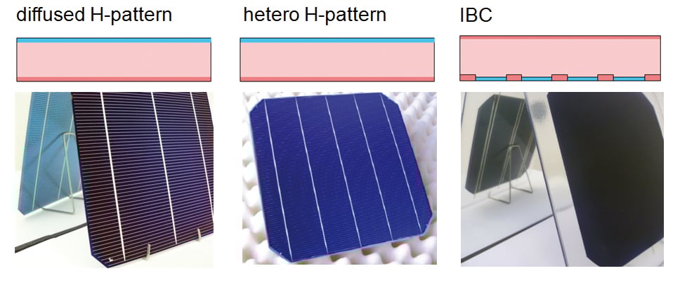
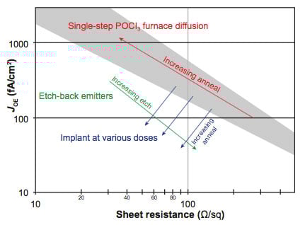
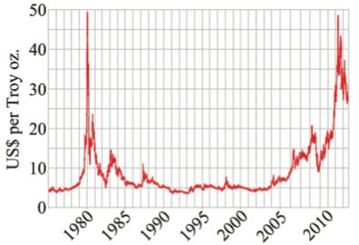
The market price of Ag has fluctuated considerably over the past ten years and has impacted the manufacturing cost of Si solar cells and the price of Si PV. Reducing Ag consumption can decrease this cost; however, such reduction may come at the expense of cell performance. In order to address the issue of Ag cost reduction while maintaining high cell efficiency, phosphorus emitter profiles are tailored via POCl3 diffusion to create solar cell emitters displaying low saturation current density (J0e), variable electrically active surface phosphorus concentration ([Psurface]), and variable sheet resistance with the aim of reducing Ag consumption. By optimizing emitter diffusion conditions, it is possible to reduce screen-printed Ag paste consumption by 33% with no loss in cell performance. Using a screen-printable Ag conductor paste designed to contact low [Psurface] emitters, the performance of cells with screen-printed Ag paste dry masses of 200, 120 and 80mg is compared. By using a tailored low-J0e 55Ω/sq emitter, it is possible to achieve a high open-circuit voltage (Voc) and short-circuit current (Jsc) to yield average cell efficiencies of 18.64% and 18.73% for 120mg and 80mg Ag paste dry mass, respectively. This is compared with efficiencies of 18.52% for cells using state-of-the-art technology (industrial high [Psurface] 65Ω/sq emitter with 120mg Ag paste dry mass). On the basis of a Ag market price of US$32/troy oz and an 85% by weight thick-film paste Ag metal content, a Ag front-side metallization cost of US¢2.11/W can be achieved by using 80mg Ag paste dry mass, which translates to a Ag cost saving of US$5.4M per year for a 500MW production line when compared with the Ag cost for state-of-the-art technology. Further cost analysis shows a 1.2% area-related balance of system (BOS) cost reduction and a US¢0.1/kWh reduction when comparing low-J0e 55Ω/sq modules and state-of-the-art modules. Calculations show that an additional 0.5% absolute efficiency for state-of-the-art modules is required, to compensate the efficiency gains and Ag cost reduction afforded by low-J0e 55Ω/sq modules.
Premium
Cell Processing, Photovoltaics International Papers
The development of a cost-effective and industrially up-scalable process for p-type Cz monocrystalline silicon solar cells of the passivated emitter, rear locally diffused (PERL) type requires a careful trade-off between the potential benefits that novel process steps can deliver (in terms of improved efficiency and/or process control) and the additional costs involved. The approach chosen by Photovoltech is to limit as much as possible the number of PERL-specific process steps and to fine-tune the processes already in use for our standard full Al back-surface field (Al-BSF) technology in order to satisfy the more stringent requirements of PERL technology. Some of the results of this development are reported in this paper. In particular, the impact of different local BSF pastes on our proprietary extended laser ablation (ELA) rear-contacting technique is investigated, as well as the effect of the wafer resistivity and emitter diffusion/oxidation processes on cell performance. This paper also reports the results of large-batch experiments in which the capability of our optimized PERL process was tested against that of a standard full Al-BSF process. An average efficiency of 19.5% and a top efficiency of 19.7% were demonstrated.
Premium
Cell Processing, Photovoltaics International Papers
The passivated emitter and rear cell (PERC) is considered to be the next generation of industrial-type screen-printed silicon solar cell. However, only a few deposition methods currently exist for rear passivation layers which meet both the high-throughput and low-cost requirements of the PV industry while demonstrating high-quality surface passivation properties. This paper presents an evaluation and the optimization of a novel deposition technique for AlOx passivation layers, applying an inductively coupled plasma (ICP) plasma-enhanced chemical vapour deposition (PECVD) process. High deposition rates of up to 5nm/s, as well as excellent surface recombination velocities below 10cm/s after firing, are possible using this ICP AlOx deposition process. When applied to PERC solar cells the ICP AlOx layer is capped with a PECVD SiNy layer. Independently confirmed conversion efficiencies of up to 20.1% are achieved for large-area 15.6cm x 15.6cm PERC solar cells with screen-printed metal contacts and ICP AlOx/SiNy rear side passivation on standard boron-doped Czochralski-grown silicon wafers. The internal quantum efficiency (IQE) reveals an effective rear surface recombination velocity Srear of 110±30cm/s and an internal rear reflectance Rb of 91±1%, which demonstrates the excellent rear surface passivation of the ICP AlOx/SiNy layer stack. Currently, the ICP AlOx deposition process is being transferred from the ISFH laboratory-type tool to the Singular production tool of Singulus Technologies in order to commercialize this novel deposition process during 2012.
Premium
Cell Processing, Photovoltaics International Papers
This paper reviews metal wrap through (MWT) solar cell and module technology. As MWT solar cells and modules have received more and more attention in recent years, many highly efficient MWT cell types have been presented by research institutes and industry and are summarized herein. The MWT cell structure benefits from a reduced silver consumption compared with a conventional H-pattern cell, and its realization can be easily combined with novel metallization technologies such as dispensing or stencil printing. The introduction of a rear-surface passivation into the MWT structure is feasible with the high-performance MWT (HIP-MWT) concept developed at Fraunhofer ISE. The resulting fabrication sequence includes only one additional process step – laser drilling of vias – compared with an H-pattern passivated emitter and rear cell (PERC). Furthermore, the synergistic effects of MWT and PERC boost the conversion efficiency gain of MWT-PERC-type cells beyond the expected sum of what could be achieved individually from these two approaches. According to the calculations made by Fraunhofer ISE, conversion efficiencies of up to 21.5% (annealed) are feasible for p-type Cz silicon MWT-PERC cells. Because via metallization is one of the challenges in the fabrication of MWT cells, different via pastes are investigated with regard to their series resistance and contact behaviour. With cell-to-module losses in conversion efficiency of only 0.9% abs., both the interconnector-based MWT module technology and the conductive backsheet concept show promising results.

Subscribe to Newsletter

Upcoming Events

Media Partners, Solar Media Events
April 23, 2025
Fortaleza, Brazil
Solar Media Events
April 29, 2025
Dallas, Texas
Media Partners, Solar Media Events
May 7, 2025
Munich, Germany
Solar Media Events
May 21, 2025
London, UK
Solar Media Events
June 17, 2025
Napa, USA