Cell Processing

Premium
Cell Processing, Photovoltaics International Papers
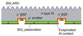
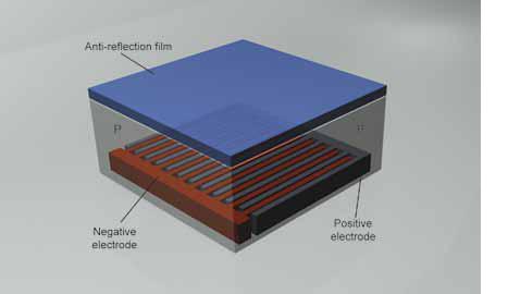
This paper presents ISFH’s recent developments and advances in the field of back-contacted silicon solar cells. The efficiency potential of back-contacted solar cells is very high; nevertheless, in industrial production, back-contacted solar cells are decidedly the minority. In the field of back-contacted solar cells, ISFH has developed several cell concepts and new processing techniques, such as laser ablation for silicon structuring, contact opening through passivation layers, and hole drilling for emitter-wrap-through (EWT) solar cells. The latest results are presented regarding ISFH’s work on back-junction back-contacted solar cells and EWT solar cells, as well as on back-contacted solar cells employing an amorphous/crystalline silicon heterojunction. Also discussed are the advances in high-throughput evaporation of aluminium as a low-cost option for the metallization of back-contacted solar cells. Finally, a novel, silver-free cell interconnection technique is presented, which is based on the direct laser welding of a highly conductive, low-cost Al foil, as a cell interconnect, onto the rear side of back-contacted solar cells.
Premium
Cell Processing, Photovoltaics International Papers
Wet chemical process equipment is widely used in industrial solar cell production, and inline etching systems in particular have attracted more and more attention since their introduction 10 years ago. The horizontal wafer transport within these systems has made it possible to think about single-side wafer treatments even for wet chemical process applications. Since its market introduction in 2004, the chemical edge isolation process based on the single-side removal of the parasitic emitter at the rear side of the solar cells has gained an increasing share of the market in comparison to competing technologies that use laser techniques. However, stabilization and control of such a process under mass production conditions remains challenging. The introduction of new high-efficiency cell concepts involving passivated rear sides will increase the importance of single-side wafer treatments, as the final solar cell performance is significantly affected not only by the complete removal of the parasitic emitter but also by an ideally polished surface on the rear side of the wafer.
Premium
Cell Processing, Photovoltaics International Papers
Texturization of (100) monocrystalline silicon (mono-Si) for solar cells is still an issue in the industrial production of standard screen-printed mono-Si solar cells. This fact is due to the properties of isopropyl alcohol (IPA), which is used together with potassium hydroxide (KOH) in the standard etching solution KOH-IPA (or used with sodium hydroxide NaOH in NaOH-IPA). The low boiling point of IPA (82.4°C) limits the etching temperature and thus the processing speed. Furthermore, KOH-IPA etching solution is very sensitive to the wafer pre-treatment characteristics of as-cut mono-Si wafers. Two ways to overcome these disadvantages are presented in this paper. The first approach involves the use of a high boiling alcohol (HBA) instead of IPA in the standard KOH-IPA etching solution. This allows higher etching temperatures to be used, without evaporation losses of the alcohol, but with reduced etching times. The second approach consists of using a closed etching bath in which vacuum (low-pressure) steps (i.e. pressure oscillations between atmospheric and below-atmospheric pressure) are achievable; in addition, a cooling system located on top of the etching bath allows the liquefaction of the evaporated IPA. The second texturing approach considerably decreases the etching time of mono-Si wafers. Examples of mono-Si wafers were textured using the new KOH-HBA etching solution and then processed into solar cells; the current-voltage results of the processed solar cells are presented.
Premium
Cell Processing, Photovoltaics International Papers
The selective emitter (SE) concept features two different doping levels at the front surface of the cell. Both doping profiles are tailored individually to best suit their specific purposes, thus achieving both low contact resistance of the emitter electrode and low recombination in the emitter and at the Si/SiNx:H interface. This paper details the experience gained since the first tools for generating an SE structure were installed two years ago. The approach taken is discussed and a presentation given of the physical concept and properties of SE technology, along with the different aspects that have to be considered when integrating SE into an otherwise unchanged production facility.
Premium
Cell Processing, Photovoltaics International Papers
In the photovoltaics industry, contacts to crystalline silicon are typically formed by the firing of screen-printed metal pastes. However, the stability of dielectric surface passivation layers during the high-temperature contact formation has turned out to be a major challenge for some of the best passivating layers, such as intrinsic amorphous silicon. Capping of well-passivating dielectric layers by hydrogen-rich silicon nitride (SiNx), however, has been demonstrated to improve the thermal stability, an effect which can be attributed to the atomic hydrogen (H) diffusing out of the interface during firing, and passivating dangling bonds. This paper presents the results of investigations into the influence of two different dielectric passivation stacks on the firing stability, namely SiNy/SiNx (y < x) and Al2O3/SiNx stacks. Excellent firing stability was demonstrated for both stack systems. Effective surface recombination velocities of < 10cm/s were measured after a conventional co firing process on 1.5Ωcm p-type float-zone silicon wafers for both passivation schemes. On the solar cell level, however, better results were obtained using the Al2O3/SiNx stack, where an efficiency of 19.5% was achieved for a large-area screen-printed solar cell fabricated on conventional Czochralski-grown silicon.
Premium
Cell Processing, Photovoltaics International Papers
Coupled device and process simulation tools, collectively known as technology computer-aided design (TCAD), have been used in the integrated circuit industry for over 30 years. These tools allow researchers to quickly home in on optimized device designs and manufacturing processes with minimal experimental expenditures. The PV industry has been slower to adopt these tools, but is quickly developing competency in using them. This paper introduces a predictive defect engineering paradigm and simulation tool, while demonstrating its effectiveness at increasing the performance and throughput of current industrial processes. The impurity-to-efficiency (I2E) simulator is a coupled process and device simulation tool that links wafer material purity, processing parameters and cell design to device performance. The tool has been validated with experimental data and used successfully with partners in industry. The simulator has also been deployed in a free web-accessible applet, which is available for use by the industrial and academic communities.
Premium
Cell Processing, Photovoltaics International Papers
This paper presents examples of recent process developments at ECN in silicon solar cells on n-type monocrystalline base material. For all PV manufacturers, the challenge is to increase module efficiencies while maintaining low production cost. An effective way to move to higher and more stable efficiencies, using low-cost industrial-type processing, is n-type solar cell technology. The solar cell considered in this paper is the n-pasha cell – a bifacial solar cell with homogeneous diffusions and screen-printed metallization. The n-pasha cell is currently produced on an industrial scale by Yingli Solar; in 2011 a maximum solar cell conversion efficiency of 19.97% was obtained using this cell concept on 239cm2 n-type Cz at the ECN laboratory. The focus of the paper will be increasing efficiency by optimization of the cell process, in particular the front-side metallization, and by improvements to the rear-surface passivation. These two steps have contributed an increase in efficiency of 0.8%, allowing cell efficiencies of 20% to be reached.
Premium
Cell Processing, Photovoltaics International Papers
Crystalline silicon wafer technology currently dominates industrial solar cell production. Common devices feature opposing electrodes situated at the front and the rear surface of the wafer, and subsequent front-to-rear interconnection is used for module assembly. This paper describes the status and perspectives of the emitter wrapthrough (EWT) cell concept, which is a fully back-contacted solar cell. The functions which have to be fulfilled for this concept, as well as the corresponding challenges and advances, are discussed.
Premium
Cell Processing, Photovoltaics International Papers
A new production process for crystalline silicon (c-Si) solar cells, specifically p-type back-contact solar cells, is proposed. In contrast to the conventional c-Si solar cell manufacturing method, this new technology eliminates the etching process and reduces the industrial three-step electrode printing to only one step, greatly improving the technological process. Furthermore, the proposed process is also largely compatible with a traditional c-Si solar cell production line. Oxidation technology for producing the SiO2 film on a c-Si wafer, together with corrosive window technology, such as through HF corrosive paste screen printing, for creating the patterning on the wafer covered with SiO2 film, are used in the fabrication of the p-type back-contact solar cells.
Premium
Cell Processing, Photovoltaics International Papers
In the photovoltaic industry, laser edge isolation (LEI) is a well-established process at the end of the process chain. However, because the cell properties vary from one cell producer to the next, no systematic approach is defined in industry for establishing an efficient isolation groove. Nevertheless, a general approach has to be defined for analyzing the LEI process for silicon solar cells. Besides the material aspects and laser parameters, atmospheric boundary conditions must be considered. This paper presents investigations into the ablation of a specific type of mc-silicon solar cell, and the most suitable laser, as well as the ambient parameters, is determined based on the results of the experiments.

Subscribe to Newsletter

Upcoming Events

Media Partners, Solar Media Events
April 23, 2025
Fortaleza, Brazil
Solar Media Events
April 29, 2025
Dallas, Texas
Media Partners, Solar Media Events
May 7, 2025
Munich, Germany
Solar Media Events
May 21, 2025
London, UK
Solar Media Events
June 17, 2025
Napa, USA