Cell Processing

Premium
Cell Processing, Photovoltaics International Papers
Al2O3 deposition has received a lot of attention in the last few years for its attractive passivation properties of c-Si surfaces. Within the local Al back-surface field (BSF) cell concept, we considered several avenues of study: surface preparation, thermal stability, charge investigation and the ‘blistering’ phenomenon. The investigations converged on a passivation stack that includes a thin interfacial SiO2 like layer and a thin Al2O3 layer (~10nm), which undergoes a high-temperature anneal (> 600°C). In order for a surface passivation with Al2O3 to be a cost-effective step for the PV industry, a high Al2O3 deposition rate is required. Compared to the different high-throughput tools that have recently emerged on the PV market, such as atomic layer deposition (ALD) and plasma-enhanced chemical vapour deposition (PECVD), our tool screening revealed quite similar results. The differences therefore seem to have an origin primarily in the tool specifications rather than in the achievable Al2O3 material properties.
Premium
Cell Processing, Photovoltaics International Papers
The need for higher efficiency solar cells is becoming more and more urgent nowadays in the photovoltaic industry. In this paper, a new method of increasing efficiency is described whereby SiN is coated by a special commercial chemical after the final step of manufacturing, which is screen printing. No mask is required for this method, but a drying temperature of 200–400°C is mandatory to activate the SiN layer. It is shown that the efficiency of a crystalline solar cell can be increased by at least 0.16% (absolute value) on average. At the same time, modules made from these solar cells do not degrade after sun exposure, and have the potential to pass the stringent standards of a potential-induced degradation (PID) test. The total cost for all the equipment and the chemical is around US$300,000 for retrofitting two (30MW each) production lines.
Premium
Cell Processing, Photovoltaics International Papers
To make solar energy cost effective, the photovoltaic (PV) industry has to reduce its manufacturing costs well below 1€/Wp. To reach this cost target, roadmaps for c-Si technology foresee a drastic reduction in the amount of high-purity Si used and an increase in solar cell efficiencies beyond 20%. But this requires advanced cell concepts that put more stringent requirements on process steps such as doping, cleaning and surface passivation. Several processes in the technology and analysis toolbox of microelectronics offer opportunities to meet these stringent requirements. In this paper, we give examples of recent progress in solar cell development that has been achieved by implementing CMOS-like process steps, and we discuss how these processes can be attuned to the needs and benefits of the solar industry.
Premium
Cell Processing, Photovoltaics International Papers
Approximately 80% of today’s silicon solar cells industrially manufactured worldwide apply screen printing for the metallization of the silver front and aluminium rear contacts. In production, conversion efficiencies of ~18–18.5% are achieved using monocrystalline silicon wafers. A baseline process has been implemented at ISFH that is very similar to the industry-standard process, displaying conversion efficiencies of up to 18.5%. An analysis of the solar cells reveals that the conversion efficiency is limited in particular by the shadowing loss due to the silver front-side metallization, as well as infrared light being absorbed in the aluminium rear-side metallization. This paper summarizes recent developments at ISFH that resulted in a 19.4% efficient large-area screen-printed solar cell, when applying a print-on-print silver front-side metallization and an SiO2/SiNx rear-surface passivation.
Premium
Cell Processing, Photovoltaics International Papers
In a multicrystalline silicon (mc-Si) cell production process, acid texturing is the most popular way of carrying out surface texturing. In general, the surface reflectivity and etch depth are the criteria used for quantifying the texture quality. In this study, four groups of cells were created with different etch depths of 2.82μm, 3.83μm, 4.41μm and 5.92μm. It was found that the etch depth had a notable effect on the efficiency of a cell. Also, the best texture was obtained with an etch depth of 4.41μm, at which there was a balance between a low reflectance and the removal of the saw-damage layer. As the etch depth increased, the film deposition thickness and the front bus-bar tensile strength were seen to increase. However, no linear relationship was found to exist between the diffusion sheet resistance and the etch depth.
Premium
Cell Processing, Photovoltaics International Papers
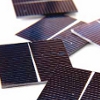
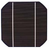
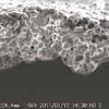
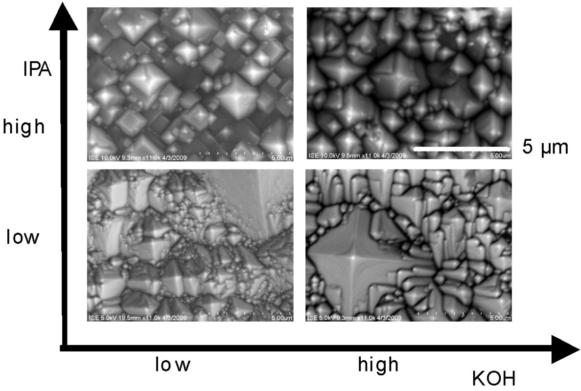
Quality assurance and process control are becoming increasingly important in the industrial production chain to the manufacturing of silicon solar cells. There are a number of relevant wet chemical processes for the fabrication of standard screen-printed industrial solar cells, mainly for texturization and cleaning purposes. While one-component systems like pure HF for oxide-removal are easy to monitor, i.e., by conductivity measurements, typical texturization processes are much more complex due to the number of constituents. For acidic texturization of multicrystalline silicon wafers, typical mixtures involve amounts of hydrofluoric acid (HF), nitric acid (HNO3) and water. It has also been documented that mixtures can be found where additional additives like phosphoric acid (H3PO4), acetic acid (HOAc) and sulphuric acid (H2SO4) have been used [1, 2]. In alkaline random pyramid texturization for monocrystalline wafers, a base like potassium hydroxide (KOH) or sodium hydroxide (NaOH) and organic additives like 2-propanol (IPA) are used [3]. In addition to these processes, recently developed high-efficiency cell concepts require several additional wet chemical process steps like advanced cleaning processes, chemical edge isolation or single side oxide removal processes [4]. In order to obtain continuously stable and reproducible process results and to overcome process operations based on operator experience, a reliable monitoring of the bath concentrations is essential. Such quality control has the potential for significant cost reductions due to optimized durations between replacements of bath mixtures or shortening of processing times. In this context, the application of on-line analytical methods, either by means of chemical, optical or electrical measurement techniques, is of particular interest.
Premium
Cell Processing, Photovoltaics International Papers
Phosphorus dopant pastes are an attractive alternative to the conventional phosphorus oxychloride (POCl3) dopant source for emitter processing in solar cells, as they allow the fabrication of selective emitters on an industrial scale. In this paper it is demonstrated that single-sided uniform screen-printed emitters, processed with phosphorus dopant pastes, can getter multicrystalline silicon (mc-Si) wafers more effectively than conventional double-sided uniform POCl3 emitters. This result is confirmed by minority carrier lifetime measurements with the quasi-stead-state photoconductance (QSSPC) method. Solar cells with selective emitters were processed using phosphorus dopant pastes on mc-Si wafers and were subsequently characterized. The current-voltage (I-V) results are improved compared to uniform POCl3 emitter solar cells and an increased internal quantum efficiency (IQE) for selective emitter solar cells is demonstrated.
Premium
Cell Processing, Photovoltaics International Papers
Technology computer-aided design (TCAD) is pervasive throughout research, development and manufacturing in the semiconductor industry. It allows very low-cost evaluation of process options and competing technologies, guides process development and transfer to production and supports more efficient process improvement with minimal down time in the factory environment. This paper reviews the use of TCAD in the semiconductor industry and shows, with some illustrative examples, its important enabling role for the PV industry.
Premium
Cell Processing, Photovoltaics International Papers
Processing silicon substrates for PV applications involves texturing, cleaning and/or etching wafer surfaces with chemical solutions. Depending on the cleanliness of the industrial equipment and the purity of the chemical solutions, surface contamination with metals or organic residues is possible [1]. The presence of trace contamination at PV junctions leads to both mid-level traps and photonic defects, which ultimately cause reduced efficiency and rapid cell degradation. Metallic impurities have a greater impact on PV cell lifetime due to their deeper energy levels in the silicon band gap [2]. On the other hand, non-metallic impurities may modify the electrical activity of PV cells because these species involve complex interactions with the host silicon lattice and its structural defects. In other words, very small amounts of contamination can result in poor PV efficiency. This paper presents an overview of the effects of adding a biodegradable complexing agent in cleaning and rinsing baths to minimize surface contamination and thereby enhance solar cell efficiency.
Premium
Cell Processing, Photovoltaics International Papers
This paper reviews the status of solar cell technology based on n-type crystalline silicon wafers. It aims to explain the reasons behind the strong and increasing attention for n-type cells, including the inherent advantages of n-type base doping for high diffusion length, and for the industrialization of designs with good rear-side electronic and optical properties. The focus will be on cells using diffused junctions.

Subscribe to Newsletter

Upcoming Events

Media Partners, Solar Media Events
April 23, 2025
Fortaleza, Brazil
Solar Media Events
April 29, 2025
Dallas, Texas
Media Partners, Solar Media Events
May 7, 2025
Munich, Germany
Solar Media Events
May 21, 2025
London, UK
Solar Media Events
June 17, 2025
Napa, USA