Cell Processing

Premium
Cell Processing, Photovoltaics International Papers
The key to delivering highly efficient solar cells is to absorb as much light as possible from the solar spectrum and convert it effectively into electrical energy. Anti-reflective coatings have served as agents for reducing reflective losses and improving bulk and surface passivation thus enhancing both of the parameters – short circuit current and open circuit voltage of a solar cell. Simulation studies show that an SiN/MgF dual-layer anti-reflective coating is best for a bare cell. This paper takes a closer look at how this coating can reduce the reflectance for a broad range of wavelengths and thus enhance the quantum efficiency of the cell in the blue and red region of the solar spectrum.
Premium
Cell Processing, Photovoltaics International Papers
Despite the fall in silicon prices, wafer thickness continues to be reduced. The handling of thin wafers between 120 and 160µm is under research at the Fraunhofer IPA, where gripper-dependent and independent variables were determined as parameters for the handling process. Diverse grippers are tested on an automated test platform. Among these are grippers that are specifically designed for wafer handling, as well as others that are not but are used for wafer manipulation. The test platform includes several different test and handling equipments and utilizes critical parameters that might be required for achieving a high production rate via shortest cycle times to investigate the impact on thin wafers. The first results of the position accuracy measurement in relation to the physical movement parameters and other industrial key figures in ongoing handling research are presented within this paper.
Premium
Cell Processing, Photovoltaics International Papers
Lowering the cost of production of solar cells requires higher throughputs and higher production yields for thinner and more fragile silicon wafers, and inline processing could hold the key. However, current processes used in production do not enable full inline processing and often require a substantial amount of handling between process stations as the throughputs per station and tray requirements differ greatly. It will take many years before a full inline process flow is available and if it comes, wafers will most likely be positioned on a single tray throughout all process stations. This paper will discuss the current processing methods for all individual process steps and will provide an outlook on inline processing in view of the three cost reduction strategies: thinner wafers, higher throughput, and higher efficiency cell designs.
Premium
Cell Processing, Photovoltaics International Papers
Laser doping is discussed often in relation to silicon photovoltaic cell efficiency enhancement. However, the specific use of lasers for dopant diffusion falls within a broader category of ‘Laser-Assisted Selective Emitters’. Understanding the benefits enabled by laser tools here is important not just in explaining what laser doping is, but why laser processing features in most selective emitter concepts.
Premium
Cell Processing, Photovoltaics International Papers
Wet processing can be a very high performing and cost-effective manufacturing process. It is therefore extensively used in Si solar cell fabrication for saw damage removal, surface texturing, cleaning, etching of parasitic junctions and doped oxide glass. PV manufacturers have succeeded in bringing down the cost of ownership of batch-type and in-line tools. The trend to back-side passivated solar cells requires cost-effective single-sided processing solutions. With the future pointing to ever-thinner silicon solar cells, handling these thin wafers in wet environments is a major challenge for any wet process. This paper reviews the major wet processing steps, emphasising some new developments and unknown issues, and provides a more general outlook on trends in wet processing.
Premium
Cell Processing, Photovoltaics International Papers
Explosive growth in sales of critical subsystems and components for use in photovoltaic manufacturing equipment provided one of the few bright spots in an otherwise depressed market during 2008. The outlook for sales into the PV industry in 2009 is for demand to be relatively flat, but strong underlying demand for PV cells should lead to a recovery in 2010 and a return to double-digit growth rates, as outlined in this paper.
Premium
Cell Processing, Photovoltaics International Papers
Amorphous silicon is one of the most effective materials in passivating silicon interfaces. At Fraunhofer ISE, highly passivating amorphous silicon coatings were developed by an industrially applicable Plasma-Enhanced Chemical Vapour Deposition (PECVD) process. Thin-film stacks of amorphous silicon and SiOx display excellent passivation quality, indicated by effective charge carrier lifetimes ranging from 900 to 1600µs and resulting surface recombination velocities between 9 and 3cm/s-1. The demonstrated temperature stability opens up new application opportunities also for amorphous silicon films in the industrial production of highly efficient solar cell structures, which will be further discussed in this paper.
Premium
Cell Processing, Photovoltaics International Papers
The principal paths to cost reduction for the photovoltaics industry are increasing the efficiency of solar cells and the power density of modules, together with the reduction of the specific consumption of silicon. Following the slowdown in the ever-increasing growth of the PV market earlier this year, and the reduction in the market cost of polysilicon, wafer producers and most cell producers moved back to the 180µm generation substrates. It may take some time for manufacturers to tackle the technological issues that need to be addressed in order to successfully decrease wafer thickness further. In this article, some of the issues related to the production of thinner and thinner cells are outlined and discussed.
Premium
Cell Processing, Photovoltaics International Papers
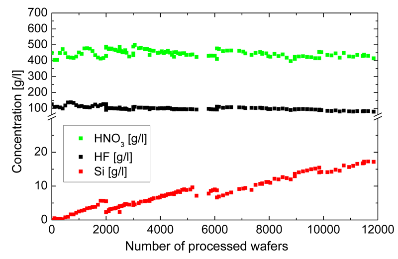
Crystalline silicon solar cell fabrication involves many wet chemical process steps. Like most processes in solar cell manufacturing, many of these wet chemical processes were transferred from the semiconductor industry. In contrast to microchip fabrication with maximum throughputs of 100 wafers/hour, state-of-the-art solar cell equipment relies on several 1000 wafers/hour. Furthermore, specific processes have been developed for the texturisation of the wafer surface. Therefore, there is a need for dedicated methods of characterization of these wet chemical processes. Fraunhofer ISE has developed several analytical methods such as titration, ion chromatography and near infrared (NIR) spectroscopy for the complete analysis of the chemical composition of wet chemical processes baths. These methods were compared considering the inline/online capability, measurement cycle and running costs, with the result that NIR spectroscopy was identified as a complex but very powerful tool for process characterization, as outlined in this paper.
Premium
Cell Processing, Photovoltaics International Papers
Formation of the pn-junction for charge carrier separation is one of the key processes of a modern high-volume solar cell production. In silicon wafer-based solar cell technology this is achieved by diffusion of phosphorus atoms in boron pre-doped wafers forming a sub-micron shallow n-type emitter in a 200µm-thick p-type base. In this contribution we discuss both the characteristics of emitter doping profiles and the diffusion process itself as required for optimal solar cell conversion efficiencies. In addition we give an overview on state-of-the-art industrial diffusion technologies and conclude with a brief outlook on their evolution.

Subscribe to Newsletter

Upcoming Events

Media Partners, Solar Media Events
April 23, 2025
Fortaleza, Brazil
Solar Media Events
April 29, 2025
Dallas, Texas
Media Partners, Solar Media Events
May 7, 2025
Munich, Germany
Solar Media Events
May 21, 2025
London, UK
Solar Media Events
June 17, 2025
Napa, USA