Cell Processing

Premium
Cell Processing, Photovoltaics International Papers
This paper gives an overview of the application of silicon epitaxy as a doping technology in bulk crystalline silicon solar cells. The large degree of flexibility in designing a doped profile in one process step, and the elegant way of locally creating doped regions, or simply achieving single-side doping by selective epitaxy, are presented. Other advantages – such as the absence of subsequent steps to drive in the doped region, to activate the dopants and to heal any damage or remove glassy layers – position the technology as a strong alternative to classical diffusion. Silicon epitaxy is possible on the flat and textured surfaces of solar material, and is compatible with cleaning sequences suited to industrial implementation. The integration of epitaxial layers in solar cells is capable of providing not only high efficiencies but also simplifications of the cell fabrication process, and, therefore, reductions in the cell cost of ownership (CoO). The proof of concept at the cell level has been demonstrated by the integration of boron-doped epitaxial emitters in n-type IBC and PERT solar cells: 22.8% efficiency for IBC (4cm2) and 21.9% for PERT (238.9cm2) devices have been obtained.
Premium
Cell Processing, Photovoltaics International Papers
Ion implantation offers significant process simplification potential for the fabrication of back-junction back-contact (BJBC) solar cells. First, the number of high-temperature steps can be reduced to one when applying a co-annealing process which includes an in situ growth of a silicon oxide passivation layer. Second, the implanted regions can be patterned in situ by utilizing shadow masks. ISFH's results from evaluating both aspects are reported in this paper. With fully ion-implanted, co-annealed and laser-structured small- area cells, efficiencies of up to 23.41% (20mm x 20mm designated area) have now been achieved. It is shown that the excellent recombination behaviour of 156mm x 156mm BJBC cells patterned in situ implies a potential for realizing efficiencies greater than 23%; however, back-end issues have so far limited the efficiency to 22.1% (full-area measurement). Ion implantation can also be utilized for the doping of BJBC cells with carrier-selective junctions based on polycrystalline silicon. The current status of ISFH's work in this direction is presented.
Premium
Cell Processing, Photovoltaics International Papers
This paper presents the main features of imec’s n-PERT (passivated emitter rear totally diffused) cells, which have achieved independently confirmed efficiencies of 22%. A special focus is given to the selective front-surface field formation by laser doping, which – combined with imec’s front-plating sequence and the excellent rear-surface passivation by Al2O3 on the boron-diffused emitters – has enabled very high voltages (close to 685mV) to be realized on large-area n-type Cz material.
Premium
Cell Processing, Photovoltaics International Papers
This paper reports on the status of large-area, 156mm, bifacial, n-type passivated emitter and rear totally diffused (n-PERT) solar cells, which feature full-area homogeneous doped regions on the front and rear sides. The fabrication process includes either two separate gas-phase diffusion processes with sacrificial diffusion barrier layers, or a sophisticated co-diffusion approach, in which a deposited stack of borosilicate glass (BSG) and silicon oxide acts as a dopant source during back-surface field (BSF) formation in a tube furnace. Thus, the co-diffusion approach reduces the number of required high-temperature processes to one, which significantly streamlines the process sequence. It is shown that by implementing two deposition phases during the BSF diffusion process, it is possible to separately control both the depth and the surface concentration of the BSF. The use of a tailored BSG source allows low recombination and specific contact resistance values on both the front and rear sides, resulting in peak conversion efficiencies of 19.9%. A discussion on the recombination at the emitter -metal interface completes the paper, and several paths to driving the conversion efficiency towards 22% are outlined.
Premium
Cell Processing, Photovoltaics International Papers
A recent revitalization of the passivated emitter and rear cell (PERC) concept in the silicon PV industry has resulted in solar energy conversion efficiencies of greater than 20% being achieved on p-type solargrade single-crystalline silicon (mono-Si) wafers during the past two years or so, thanks to technological advance in the use of aluminium oxide for silicon surface passivation. The research efforts carried out at JA Solar in developing an industry version of PERC cells that can be mass produced utilizing the existing conventional back-surface field (BSF) cell manufacturing platform with moderate retrofitting have yielded 20.5% average conversion efficiency, which can be consistently achieved on p-type Si wafers grown by the Czochralski method. Moreover, the experimental results showed that an average conversion efficiency of 20% is achievable when, in combination with JA Solar’s proprietary light-trapping technique, the same technological approach is applied to the cells using high-quality polycrystalline silicon (multi-Si) wafers produced by the seeded directional solidification method.
Premium
Cell Processing, Photovoltaics International Papers
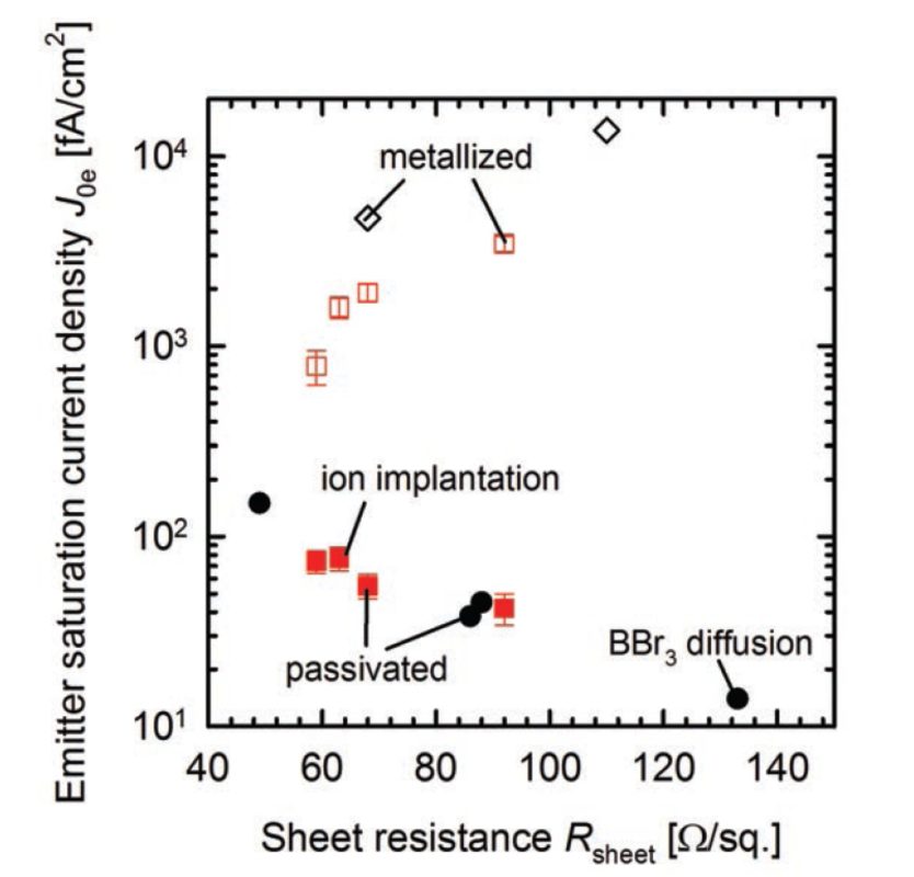
In this paper large-area (239cm2) n-type passivated emitter, rear totally diffused (n-PERT) solar cells are compared with state-of-the-art p-type passivated emitter and rear cells (p-PERC) to evaluate potential advantages of n-PERT over p-PERC. In particular, an investigation has been carried out of fully screenprinted bifacial n-PERT solar cells, in which the boron-doped emitter is contacted with aluminiumcontaining silver (AgAl) pastes, as well as of n-PERT back-junction (BJ) solar cells, in which the B-doped emitter is locally contacted with screen-printed Al. Using two separate quartz furnace diffusions for the B- and P-doped regions, efficiencies of up to 20.3% on bifacial n-PERT solar cells and of up to 20.5% on n-PERT BJ solar cells were achieved. In comparison, reference p-PERC solar cells that were processed in parallel achieved efficiencies of up to 20.6% before light-induced degradation (LID), but degraded to 20.1% after 48 hours of illumination. In addition, ion implantation and pre-deposition of dopant sources have been evaluated as alternative technologies for forming the full-area doping of the front and rear wafer surfaces, thus reducing the number of processing steps for n-PERT solar cells. Using ion implantation and a co-annealing step, efficiencies of up to 20.6% for bifacial n-PERT solar cells have been achieved, and of up to 20.5% for n-PERT solar cells, in which the P-doped back-surface field is contacted with evaporated Al. By employing a boron silicate glass (BSG) deposited via plasma-enhanced chemical vapour deposition (PECVD) as a dopant source, along with a co-diffusion step, n-PERT BJ solar cells have been fabricated with up to 19.8% energy conversion efficiency.
Premium
Cell Processing, Photovoltaics International Papers
The aim of this paper is to dispel the common belief that bifaciality is nonsense as it is not a mature technology, it is expensive and, because in large systems there is limited albedo from the rear side, it only serves the niche market. A complete picture of bifacial cell technologies and module concepts is presented, as well as levelized cost of electricity (LCOE) results for present and future bifacial systems.
Premium
Cell Processing, Photovoltaics International Papers
This paper reports on the progress of R&D in two n-type cell and module concepts: the n-Pasha solar cell and bifacial module, and the n-MWT (metal wrap-through) cell and module. Both are part of ECN's technology platform, acting as a roadmap for research in n-type Cz cells and modules. The technology platform also encompasses low-cost IBC solar cells. In the case of n-Pasha, recent developments involve improved stencilprinted metallization, resulting in an increased Isc and Voc and efficiencies of up to 20.5%. For the bifacial module aspect, research has been done on the effect of different albedo on the module output. A gain of 20%rel in module output power was obtained with an optimized background, increasing the module power from 314W to 376W. As regards n-MWT cells, the front-side metallization pattern has been changed significantly. The number of vias for conducting the emitter current to the rear has been increased from 16 to 36, resulting in reduced lengths of busbars and fingers and consequently an increase in FF. At the same time, the metal coverage on the front side has been reduced from 5% to 3% of the total area, leading to a gain in Isc and Voc and a significant reduction in Ag consumption. All these factors will result in a lower cost/Wp. For the improved n-MWT design, average efficiencies of 20.8% over a large batch (134) of cells have been obtained, with the highest recorded efficiencies being 21.0%.
Premium
Cell Processing, Photovoltaics International Papers
This paper presents the first 60-cell module results from a very simple process scheme for creating fully plated nickel-copper contacts on crystalline silicon solar cells. Standard Cz back-surface field (BSF) cells are processed in a completely analogous way to the standard process sequence up to and including rear-side screen printing. After a firing step for BSF formation, the front-grid positions are defined by picosecond pulse laser ablation and plated with nickel, copper and silver; this is followed by a short thermal anneal. Cell classification produces a very neat efficiency distribution of 19.6±0.1%. Solder and peel testing shows this approach to be competitive with standard screen-printed contacts in terms of adhesion. A batch of 60-cell modules were fabricated from the cells in a standard automated tabber-stringer system and subjected to thermal cycling and damp heat testing as part of the IEC 61215 reliability test sequence. The modules passed the test sequence without showing any signs of electrical degradation caused by, for example, copper diffusion.
Premium
Cell Processing, Photovoltaics International Papers
The PV industry is intensively evaluating technologies for further increasing conversion efficiency while maintaining, or even further reducing, production costs. Two promising technologies that meet these objectives are 1) the passivated emitter and rear cell (PERC), which reduces optical and recombination losses of the solar cell's rear side; and 2) multi-busbar/multi-wire module interconnection, which reduces optical and resistive losses of the front grid. This paper evaluates a combination of these two technologies, in particular industrial PERC solar cells with printed metal contacts employing a five-busbar (5BB) front grid instead of the typical three-busbar (3BB) design. The resulting 5BB PERC solar cells demonstrate an independently confirmed conversion efficiency of 21.2%, compared with the 20.6% efficiency for 3BB PERC cells. To the authors' knowledge, a value of 21.2% is the highest reported so far for typical industrial silicon solar cells with printed metal front and rear contacts. The higher conversion efficiency is primarily due to an increased short-circuit current, resulting from the reduced shadowing loss of the 5BB front-grid design, in combination with stencil-printed finger widths of only 46μm.

Subscribe to Newsletter

Upcoming Events

Media Partners, Solar Media Events
April 23, 2025
Fortaleza, Brazil
Solar Media Events
April 29, 2025
Dallas, Texas
Media Partners, Solar Media Events
May 7, 2025
Munich, Germany
Solar Media Events
May 21, 2025
London, UK
Solar Media Events
June 17, 2025
Napa, USA