Cell Processing

Premium
Cell Processing, Photovoltaics International Papers
Actual solar cells are large-area, two-dimensional (2D) devices with lateral variations in internal voltage, but most of the time they are represented by simplistic equivalent circuits consisting of a few lumped elements. Griddler© is a finite-element-method (FEM) simulator that constructs and solves the full 2D distributed network representation of a metallized solar cell. Not only is this approach far more versatile and adaptable to real-world problems, accurate in predicting subtle device characteristics, and compatible with mapping data, but it can also be implemented in a way that is as easy and quick to use as a handy calculator. This paper covers a broad range of applications related to full-area 2D modelling and introduces Griddler 1.0 - a compact freeware computer program that places much of that power at the fingertips of any solar cell engineer with a PC.
Premium
Cell Processing, Photovoltaics International Papers
The combination of metal-wrap-through technology with a unit cell design, referred to as AP-MWT architecture, is proposed for the purpose of operating under low and concentrated irradiance. On the illuminated side, the negative polarity is electrically separated by using an emitter window surrounding the perimeter of each unit cell. The final functioning silicon-based device consists of an arbitrary amount of unit cells with perimeter dimensions ranging from 1cm x 2.25cm to 14cm x 13.5cm. The Czochralski-based bulk material, as well as the assembly approach, conforms with state-of-the-art industrially feasible technologies. For irradiances corresponding to 1 and 10 suns, median efficiencies of 19.8% and 20.9% and top efficiencies of 20.2% and 21.0% have been achieved. Thanks to the flexibility in size, interconnection and irradiance, awide range of current-voltage ratios are covered, providing customized solutions beyond the conventional flat-panel market.
Premium
Cell Processing, Photovoltaics International Papers
The n-Pasha n-type silicon solar cell currently achieves an average conversion efficiency of 20.2% using a relatively simple process flow. This bifacial cell concept developed by ECN is based on homogeneously doped p+ front and n+ back surfaces. To enhance the cell efficiency, it is important to reduce the carrier recombination within the boron-diffused p+ region and at its surface. This paper addresses a novel way to tune the boron-doping profile and presents advanced surface passivation schemes. In particular, it is demonstrated that a very thin (2nm) Al2O3 interlayer improves the passivation of the boron-doped surface; the Al2O3 films were deposited in industrial atomic layer deposition (ALD) reactors (batch or spatial). Moreover, it is shown that the boron-doping profile can be improved by etching back the boron diffusion. On the basis of the results presented, it is expect that n-Pasha solar cells with 21% efficiency will soon be within reach.
Premium
Cell Processing, Photovoltaics International Papers
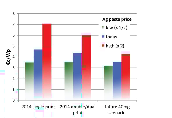
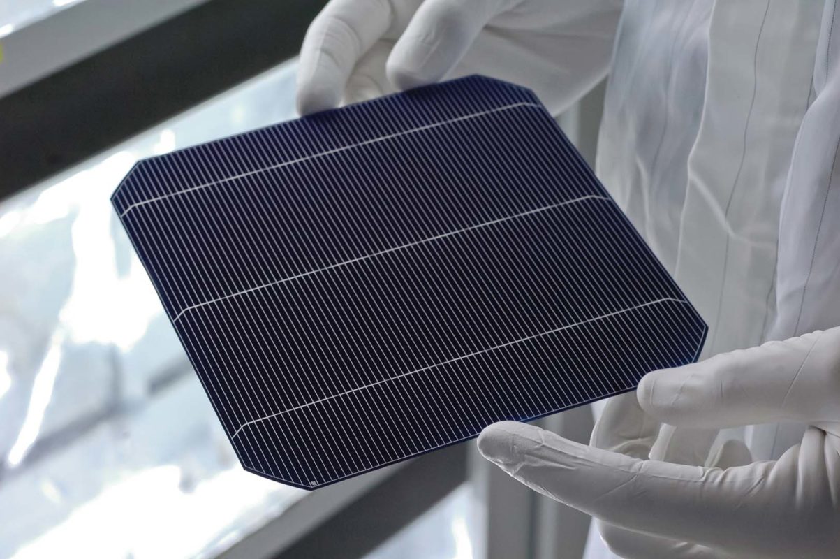
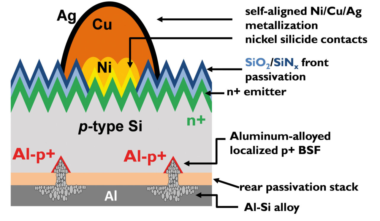
Although considerable progress has been made in reducing the amount of Ag required per wafer in the classic screen-printing metallization of Si solar cells, the total cost of ownership of the metallization process today accounts for more than 50% of the total cell-process-related cost. There has been pressure on cell and module manufacturers to further reduce this cost, by either improving the metallization process or applying alternative contacting technologies. In this paper, the classic screen printing of standard Si-based solar cells, which has been the main metallization technique for many years, is described in detail. The required paste volume for providing the contacts in a state-of-the-art cell production process is calculated on the basis of the contact dimensions (fingers and busbars on the front, Al layer and Al/Ag pads on the back). Taking into account today's paste prices, equipment investment, screen cost, energy, maintenance, yield, material utilization and necessary labour, the total cost of ownership of the cell metallization is also determined. The main cost drivers are discussed in detail. The cost reduction is estimated when improved printing processes – such as double, dual or stencil printing – are employed. Other promising alternative front-contact metallization technologies are listed and their potential is briefly discussed. To evaluate the competitiveness of these technologies, the limit of today's screen-printing method and its further cost reduction potential are estimated on the basis of the physical properties of cells and printing pastes.
Premium
Cell Processing, Photovoltaics International Papers
After several years of crisis, the PV manufacturing industry is expected to pick up again from 2014 onwards, and cell and module producers will consequently expand their production capacities in the coming years. To obtain high margins, producers must introduce new products that are better performing in terms of electrical performance and lifetime, even under harsh climatic conditions (e.g. in desert regions). This requires the use of innovative technologies that not only allow low production costs (US$/Wp), but also guarantee at the same time high module efficiencies and – even more importantly – high energy yields in terms of kWh over the entire lifetime of the system. This means that the most promising advanced cell concepts will use a limited number of standard industrial process steps and proven standard equipment. For at least the next five (probably more) years, high efficiency (>20%) at a reasonable cost will still be achieved with crystalline silicon-based technology alone. The research and development at ISC Konstanz therefore concentrates mainly on cell concepts that can be implemented using standard tube furnace diffusions and screen-printed metallization, with a focus on n-type-based technologies. This paper gives an overview of ISC Konstanz's technology zoo, including BiSoN, PELICAN and ZEBRA cell concepts, which are ready for industrial implementation. In addition, the integration of these innovative cells into modules, along with the importance of various features – such as bifaciality – in increasing the energy yield, is discussed.
Premium
Cell Processing, Photovoltaics International Papers
Over the last few years several technologies have been investigated with the aim of reducing recombination in emitters and at passivated surfaces. Because of its high efficiency potential, the passivated emitter and rear cell (PERC) design is of interest to both cell manufacturers and R&D institutes all over the world. Another cell design of interest is the metal wrap-through (MWT) solar cell, where the absence of front busbars leads to reduced shading. The MWT technology, especially when combined with rear-surface passivation, has the potential to significantly decrease the cost of ownership of today's solar cells. This paper gives an overview of the current status of the production technology for the fabrication of PERC and MWTPERC solar cells, as well as a summary of recently published papers in this field.
Premium
Cell Processing, Photovoltaics International Papers
This paper discusses the role of wafer cleaning in solar cell processing, and addresses its increasing importance with the introduction of new process steps for manufacturing high-efficiency solar cells. The requirements for cleaning before several process steps, in relationship to the solar cell production sequence, are discussed: frontend- of-the-line (FEOL) cleaning needs to reduce metal surface concentrations by several orders of magnitude (residues from wafer sawing), while back-end-of-the-line (BEOL) cleaning needs to reduce mostly process induced contamination, which tends to be much lower. A ten-step roadmap for process integration and optimization of new cleaning processes from lab to fab is suggested, which is based on process analytics and simple bath-lifetime simulations. A number of advanced cleaning steps are identified and their suitability for solar cell mass production is examined. The influence of the different input variables is demonstrated, with a focus on feed and bleed settings. Finally, the need for constant monitoring of cleaning baths is highlighted, and a device developed by Metrohm for cost-effective on-site monitoring of metallic contamination is discussed.
Premium
Cell Processing, Photovoltaics International Papers
Minimizing the breakage rate of silicon wafers and cells during production has been one of the key issues for reliable and productive solar cell manufacturing. However, the root causes of damage or breakage, as well as the mechanical characteristics of manufacturing processes, are not completely understood. In the study described in this paper the change in mechanical strength and the damaging of wafers and cells was analyzed in an industrial cell manufacturing line in order to detect critical process steps and handling operations in certain processes such as etching, diffusion, screen printing and firing. An analysis and discussion of damage sources is presented which offers more insight than the conventional study of breakage rate that is mostly performed by cell manufacturers. In a systematic experimental study, 19 different locations in the production line were investigated. The mechanical strength of 800 wafers or cells at different points in the cell line was subsequently determined using the four-line bending test and the statistical parameters for the Weibull distribution. It was discovered that dramatic changes in strength occur at different process steps because of the change in defect structure; there were also found to be several positions at which no further damage was detected. This method of investigation can therefore be used as a fingerprint of a cell line in respect of yield and breakage rates. Individual processes can be identified that indicate high damage potential, although the actual breakage could occur in a subsequent process step.
Premium
Cell Processing, Photovoltaics International Papers
This paper presents the status of imec’s work on the use of copper for the main conductor as an alternative to screen-printed silver front contacts in solar cells. This work is motivated not only by the limitations that Ag screen-printed contacts have regarding solar cell efficiency (high contact shading, limited line conductivity, and poor contact resistance to moderately doped emitters), but also by the PV industry's desire to reduce Ag usage for reasons of cost. Despite the potential advantages of Ni/Cu contacts, their commercialization has been limited because of increased process complexity and doubts over the €/Wp advantage and long-term reliability. These three factors all depend on the specific process and toolset and are discussed in this paper. A relatively simple process sequence is described that uses industrial pilot-line tools and consists of: 1) defining the front-contact pattern by ps-UV laser ablation; 2) self-aligned plating of the contacts using Ni/Cu/Ag; and, finally, 3) sintering in N2 for nickel silicidation. The process sequence is applied to 15.6 x 15.6cm2 p-type CZ-Si PERC (passivated emitter and rear cell) solar cells with 120Ω/sq. homogeneous emitters; average cell efficiencies of 20.5% are achieved over more than 100 cells. Cost analysis results are then discussed, indicating that this Ni/Cu process sequence has a lower cost/piece than equivalent screen-printed PERC cells while also providing ~0.5% abs. higher cell efficiency. Thermal-cycling and damp-heat reliability data that meet extended (1.5 x) IEC 61215 criteria for singlecell laminates and small modules are reported. The improved efficiency potential of applying this metallization sequence to rear-junction n-type PERT (passivated emitter and rear totally diffused) cells is discussed and preliminary results are given.
Premium
Cell Processing, Photovoltaics International Papers
Passivated emitter and rear cells (PERC) are considered to be a next generation of industrial solar cells, and several companies have already started pilot production. The much-reduced rear-surface recombination in PERC cells requires improvements to the front side, for example the emitter, in order to further increase the conversion efficiency in the future. This paper presents an evaluation of the emitter technologies of three industrially applicable PERC cell concepts: 1) with an ion-implanted emitter, 2) with a chemically polished rear surface, and 3) with a selective emitter formed by gas phase etch-back (GEB). The results are compared with a reference high-efficiency POCl3-diffused PERC cell. The three industrial PERC concepts utilize lean industrially applicable process flows which reduce the phosphorus concentration at the wafer surface. Accordingly, when compared with the POCl3-diffused emitter, the ion-implanted and GEB emitters obtain significantly lower emitter saturation current densities of 40 to 60fA/cm2 for emitter sheet resistances of 90 to 130Ω/sq. When applied to large-area PERC cells with screen-printed metal contacts, the ion-implanted and GEB emitter cells demonstrate up to 10mV higher open-circuit voltages than the POCl3-diffused reference PERC cell, and achieve conversion efficiencies of 20.0 and 20.3%, respectively. The next steps in further increasing the efficiency are outlined.

Subscribe to Newsletter

Upcoming Events

Media Partners, Solar Media Events
April 23, 2025
Fortaleza, Brazil
Solar Media Events
April 29, 2025
Dallas, Texas
Media Partners, Solar Media Events
May 7, 2025
Munich, Germany
Solar Media Events
May 21, 2025
London, UK
Solar Media Events
June 17, 2025
Napa, USA