Fab & Facilities

Premium
Fab & Facilities, Photovoltaics International Papers
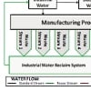
As the solar photovoltaic industry has matured from MW-scale pilot plants to large-scale mass manufacturing, costs of solar cells have steadily fallen. To further drive down costs of solar electricity beyond grid parity, a new approach that is being used is to investigate how photovoltaic manufacturing fits into the industrial ecology of a region. Optimizing the utilization of the waste associated with photovoltaic manufacturing itself and its components, while carefully considering geographic proximity, allows for industrial symbiosis. Industrial symbiosis engages traditionally separate industries in a collective approach to competitive advantage, involving physical exchange of materials, energy, water and/or by-products. Preliminary studies and industrial experimentation with co-production/co-location indicate that industrial symbiosis in photovoltaic manufacturing not only improves photovoltaic technology’s already stellar life-cycle environmental performance, but also provides for additional revenue streams that can be used to further reduce photovoltaic device costs. For example, simply coupling a glass manufacturing plant making substrates to a GW-scale amorphous silicon thin-film photovoltaic manufacturing plant, and using recycled glass where technically viable, can lead to a reduction of 30,000 tons/year in raw materials and a 12% reduction in embodied energy. Coupling the glass plant to a greenhouse to make use of waste heat means that more than 700 tons of tomatoes can be grown each year. Both these material and energy savings and additional revenue streams contribute to lowering photovoltaic manufacturing costs, which will play a progressively more important role in photovoltaic manufacturing at the large (>GW) scale.
Premium
Fab & Facilities, Photovoltaics International Papers
The low material cost and proven manufacturability of thin-film silicon has made this material very attractive for low-cost photovoltaics (PV). It is widely recognized that increasing the light-to-electricity conversion efficiency will play a critical role in expanding the acceptance of these products. The first commercial thin-film silicon solar cell consisted of a singlejunction structure using amorphous silicon; multijunction cells incorporating amorphous silicon and silicon germanium were later used to further improve efficiency. An even later development was the incorporation of nanocrystalline silicon as an active layer. This very interesting material, which consists of nanocrystallites embedded in an amorphous tissue, has already given rise to a significant increase in the performance of these multijunction cells. Most recently, some very innovative light-trapping concepts have been suggested that can improve the efficiency further. Both these topics, however, have required expertise not readily available within one organization. A thin-film silicon team has been established under a US Department of Energy’s Solar America Initiative programme to address the material, device and manufacturability issues for this technology. United Solar Ovonic is the team leader, with Colorado School of Mines, University of Oregon, Syracuse University and the National Renewable Energy Laboratory (NREL) as members. The collaborative effort has resulted in a new understanding of the material and devices; innovative light trapping ideas were developed, and worldrecord initial efficiencies of 16.3% for small-area cells and 12% for large-area encapsulated cells were reached. Of equal importance is United Solar’s decision to introduce this technology into production. This paper presents the important technical results obtained under this programme and will discuss future directions.
Premium
Fab & Facilities, Photovoltaics International Papers
Various economic and political influences continue to push high-volume manufacturing of semiconductor and PV devices into relatively arid and water-constrained geographies. As the social, economic and political focus on water resources and sustainability increases daily, the need to address the supply, use and disposal of water at manufacturing facilities is growing increasingly more complex. Historically, PV manufacturing has not been considered a major water consumer so there has been little scrutiny of water management. As the costs of water and wastewater disposal spiral upwards, water resource management becomes a significantly more important factor in the capital and operating costs of PV manufacturing. This paper outlines the preparation of a water management diagram (WMD) with reference to the development of water systems for new PV manufacturing plants, and discusses some cautionary design considerations.
Premium
Fab & Facilities, Photovoltaics International Papers
Supporting a smooth application of new wafer materials and handling equipment into photovoltaic mass production requires extensive testing of new wafers and equipments under a range of potential operating conditions. The management of such experiments, both in laboratory and production environments, demands the integration and management of a multitude of differing information. This includes static data-like equipment, specifications and experiment settings, online machine data regarding process signal and events – but also unstructured human knowledge, which is available in manual and test reports. To efficiently deal with these kind of complex environments, knowledge management techniques have proven to be a promising approach in various industrial applications. This paper depicts, by means of a photovoltaic wafer-testing platform at Fraunhofer IPA, how the application of automation systems and knowledge management techniques leads to more effective experiment management. More precisely, the gathered knowledge from the wider range of information included in the analysis of experiments can be re-used during future experiments and the manual effort is significantly reduced.
Premium
Fab & Facilities, Photovoltaics International Papers
This paper presents the Q-Cells research line (RL) as a core of the Reiner Lemoine Research Centre, including the technical set-up, the organization of the operation and current results of cell concepts processed in the RL on a regular basis. Trends of cell parameters for those processes are shown, and a focus is presented regarding the results of our high-efficiency cell concepts for multi- and monocyrstalline material processed in the RL with stabilized record efficiencies of 18.4% and 19.2%, respectively. In addition, we discuss the process flow and the results of a monitoring procedure that is used to check the rear-side passivation quality of the company’s equipment. Results of our current passivation stack show a surface recombination velocity of below Srear < 10cm/s, well suited to fabricating p-type Si solar cells with efficiencies above 20%.
Premium
Fab & Facilities, Photovoltaics International Papers
In 2006, Conergy AG started construction on one of the most advanced solar factories in the world in Frankfurt (Oder). On 35,000 square metres, a fully integrated and fully-automated wafer, cell and module production facility was created – all under one roof. Since 2008, production has been running at full speed and every day more than 3,000 premium modules roll out of the factory. This paper outlines the Manufacturing Execution System (MES) process put in place by Conergy during the planning phase of the factory, to monitor and control the complex and merging production processes.
Premium
Fab & Facilities, Photovoltaics International Papers
This article provides an overview of the typical waste water treatment methods for crystalline silicon solar cell production. Firstly, a short description is provided of the main process steps of photovoltaic production and the types of waste water generated during these steps. Secondly, the typical waste water treatment methods of hydrogen fluoride (HF) precipitation and neutralization are presented. Furthermore, some options for the reuse of rinse water are discussed and several guidelines for the design of waste water treatment systems are given. Finally, the relative environmental impact of the waste water treatment compared to the emissions of the whole fab is presented using the life-cycle assessment (LCA) methodology.
Premium
Fab & Facilities, Photovoltaics International Papers
The recent 30% decline in module market prices is the most telling sign of a need for continuous reductions in PV production costs. With this in mind, the cost efficiency of production processes is, next to stable product quality, a vital objective in the planning of production facilities. In this paper, the lessons learned in the area of cost of ownership (COO) forecasting methodologies will be analyzed and evaluated for their potential application to investment decisions in the PV industry. This paper will analyze the cost structure of the PV industry with the aim of underlining the importance of a systematic cost-of-ownership approach.
Premium
Fab & Facilities, Photovoltaics International Papers
A major challenge for the solar industry over the next few years is the reduction of production costs on the road to grid parity. Capacity must be increased in order to leverage scaling effects, production and cell efficiency must also be enhanced, and the industry must focus on intensified process optimization and quality control. Laser marking can make a key contribution to fulfilling these requirements. As hard physical coding, laser marking is applied to the raw wafer at the start of the manufacturing process, making each solar cell traceable along the entire value chain and over its whole lifetime. This paper presents Q-Cells’ laser-supported process for coding each individual solar cell (European patent pending), which will require transition work at the laboratory stage before the company’s innovation is ready for mass production.
Premium
Fab & Facilities, Photovoltaics International Papers
This paper presents and discusses the merits of layout, systems and options for exhaust treatments in PV cell production. Such treatments usually comprise central acid scrubbing, NOx scrubbing, Volatile Organic Compound (VOC) removal and several local treatments for dust, silane, and VOCs, while caustic scrubbing is an option for monocrystalline PV cell production. As direct and indirect major emissions from typical production steps have already been identified [1], this article focuses on a full emission pattern and identifies two sectors, VOC and NOx treatment, as most important for environmental impact analysis.

Subscribe to Newsletter

Upcoming Events

Media Partners, Solar Media Events
April 23, 2025
Fortaleza, Brazil
Solar Media Events
April 29, 2025
Dallas, Texas
Media Partners, Solar Media Events
May 7, 2025
Munich, Germany
Solar Media Events
May 21, 2025
London, UK
Solar Media Events
June 17, 2025
Napa, USA